sr锁存器和rs锁存器_数字电子产品中的SR锁存器
sr锁存器和rs锁存器
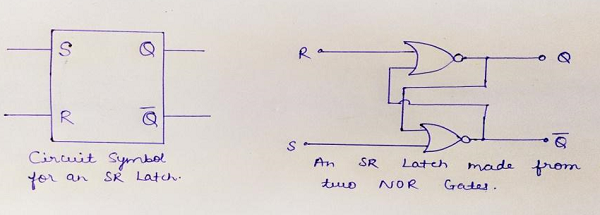
锁存器 (Latch)
The word latch means "to lock". A Latch is an example of a bistable multivibrator (the device which has two stable states). In the first stable state is the high-output and the second one is low-output. A Latch contains a feedback path from which the information can be retained by any device. So, we can conclude that latches are memory devices that are capable to store one bit of data when the power supply is provided. Designing of latches will be similar to flip-flops, but they do not have clocks.
闩锁一词的意思是“锁定” 。 锁存器是双稳态多谐振荡器(具有两个稳定状态的设备)的示例。 在第一个稳定状态下为高输出,第二个为低输出。 锁存器包含一个反馈路径,任何设备都可以通过该路径保留信息。 因此,我们可以得出结论, 锁存器是在提供电源时能够存储一位数据的存储设备 。 锁存器的设计将类似于触发器,但它们没有时钟。
SR Latch的施工和建造 (SR Latch working and construction)
SR latch (Set/Reset) works independently of clock signals and depends only upon S and R inputs, so they are also called as asynchronous devices. SR latch can be created in two ways- by using NAND gates and also can be implemented using NOR gates. SR latch created by NAND gates is sometimes called an inverted SR latch.
SR锁存器 (设置/复位)与时钟信号无关,并且仅取决于S和R输入,因此它们也称为异步设备。 SR锁存器可以通过两种方式创建- 使用“与非”门 ,也可以使用“或非”门实现。 由“与非”门创建的SR锁存器有时也称为反向SR锁存器。
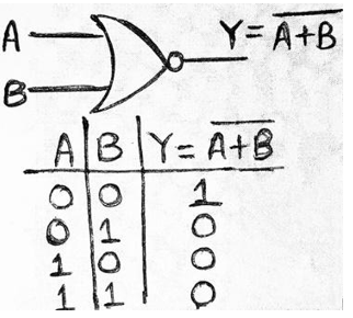
Working of SR NOR latch:
SR NOR锁存器的工作:
For understanding the working of SR NOR latch, we need to have a look at the truth table of the NOR gate (given below) which shows if any of the input is 'high' output becomes 'low', irrespective of the other input.
为了理解SR NOR锁存器的工作原理,我们需要查看NOR门的真值表(如下所示),该表显示任何输入是否为“高”输出都变为“低”,而与其他输入无关。
Case 1: When R=0 and S=0
情况1:当R = 0和S = 0时
Let us suppose, initially the value of Q be 0 then, both the inputs of lower NOR gate becomes zero, and output of that gate becomes 1 i.e., Q'=1, now in the upper gate inputs provided will be 0 and 1, so from truth table of NOR gate we know the output will be low hence Q=0.
让我们假设,最初Q的值为0,那么下或非门的输入都为零,并且该门的输出为1,即Q'= 1 ,现在在所提供的上门的输入中将为0和1。因此,根据“或非”门的真值表,我们知道输出将较低,因此Q = 0。
From this observation, we can conclude that output in the next state remains the same as the output in the previous state. This condition of the latch is known as Memory condition / Hold state / Latched state.
从这个观察结果,我们可以得出结论,下一个状态的输出与前一个状态的输出保持相同。 锁存器的这种状态称为存储状态/保持状态/锁存状态 。
Case 2: When R=1, S=0
情况2:当R = 1时,S = 0
When R=1 and S=0, then at the upper NOR gate, we will receive output as 0 i.e., Q=0, now at the lower NOR gate we have both inputs as 0, so the output Q’=1. Thus, this condition of the latch is known as Reset Condition.
当R = 1且S = 0时,在上或非门,我们将接收输出为0,即Q = 0,现在在下或非门,我们两个输入均为0,因此输出Q'= 1。 因此,锁存器的这种状态称为复位状态。
Case 3: When R=0, S=1
情况3:当R = 0时,S = 1
In this case, output at the second NOR gate will be 0 i.e., Q’=0, now at first NOR gate inputs provided will be both 0, so the output will be Q=1. Thus, this condition of latch is known as Set Condition.
在这种情况下,第二个NOR门的输出将为0,即Q'= 0,现在在第一个NOR门处提供的输入将均为0,因此输出将为Q = 1。 因此,该锁存条件称为置位条件。
Case 4: When R=1, S=1
情况4:当R = 1时,S = 1
At both gates, we will gate output Q and Q'=0, which is absurd and does not follow the basic working of latch, both Q and Q' must be complementary to each other. So, this condition of latch is known as Invalid state/Race-Around condition/Forbidden state.
在两个门处,我们将对输出Q和Q'= 0进行门操作,这是荒谬的,并且不遵循锁存器的基本工作,因此Q和Q'必须彼此互补。 因此,锁存器的这种状态称为无效状态/绕圈状态/禁止状态。
Thus, above all cases of the latch can be summarized in a truth table as:
因此,最重要的是,在真值表中可以将闩锁的所有情况总结为:
Working of SR NAND latch:
SR NAND锁存器的工作:
To understand the working of SR NAND latch, we need to have a look at the truth table of NAND gate given below.
要了解SR NAND锁存器的工作原理,我们需要查看下面给出的NAND门的真值表。
Case 1: When S=0, R=0
情况1:当S = 0时,R = 0
Let us suppose, the value of Q at the start of the circuit be 1, then inputs at the lower gate will be 1, thus from truth table of NAND gate, we can say that output of the lower gate will be 0 i.e., Q’=0, as a result, input at the upper gate will be 0 & 1. We know, if any of the inputs of the NAND gate is low, the output will always be high, thus Q=1.
让我们假设,电路开始时Q的值为1,那么下门的输入将为1,因此从与非门的真值表中,我们可以说下门的输出将为0,即Q '= 0,因此,上门的输入将为0&1。我们知道,如果“与非”门的任何输入为低,则输出将始终为高,因此Q = 1。
Therefore, we can observe the output in the next state to be the same as in the previous state. So, this condition of the latch is known as Memory state/Hold condition.
因此,我们可以观察到下一个状态的输出与上一个状态的输出相同。 因此,锁存器的这种状况称为“ 内存状态/保持状况” 。
Case 2: When S=0, R=1
情况2:当S = 0时,R = 1
The inputs provided to the lower gate is 0, thus output will be high i.e., Q'=1. Now, at the upper gate inputs provided are 1, thus output Q=0. This condition of latch is known as Reset Condition.
提供给下栅极的输入为0,因此输出将为高,即Q'= 1。 现在,在上栅极处提供的输入为1,因此输出Q = 0。 锁存器的这种条件称为复位条件。
Case 3: When S=1, R=0
情况3:当S = 1时,R = 0
In this case, one of the outputs at upper gate will be 0, thus we will get Q=1, similarly inputs at lower gate are 1 and 1, so we get output Q'=0. This condition of latch is known as Set Condition.
在这种情况下,上栅极的输出之一将为0,因此我们将得到Q = 1,下栅极的类似输入将为1和1,因此我们将获得输出Q'= 0。 锁存器的这种条件称为置位条件。
Case 4: When S=1, R=1
情况4:当S = 1时,R = 1
In this case, one of the inputs of each gate will be low, and we know if any of the inputs of the NAND gate is low its output will be high, so both Q and Q'=1, which is not possible, thus we neglect this condition. This condition of the latch is known as Invalid state / Race-Around condition / Forbidden state.
在这种情况下,每个门的输入之一将为低,并且我们知道“与非”门的任何输入是否为低,其输出将为高,因此Q和Q'= 1都是不可能的,因此我们忽略了这种情况。 锁存器的这种情况称为无效状态/比赛状态/禁止状态 。
All the above cases of the latch can be summarized in the table as:
锁存器的所有上述情况可以在表中总结为:
翻译自: https://www.includehelp.com/basics/sr-latch-in-digital-electronics.aspx
sr锁存器和rs锁存器
sr锁存器和rs锁存器_数字电子产品中的SR锁存器相关推荐
- multism中ui和uo应该怎么表示_Multisim在模拟与数字电子技术中的应用(最终版)最新版...
<Multisim在模拟与数字电子技术中的应用.doc>由会员分享,可免费在线阅读全文,更多与<Multisim在模拟与数字电子技术中的应用(最终版)>相关文档资源请在帮帮文库 ...
- 电子产品中EMC隔离设计的方法
目录 1.隔离分类 2.EMC中隔离分析 2.1.光耦隔离 2.2.继电器隔离 2.3.共模扼流圈(共模电感)隔离 在电子产品设计中,为了截断产品内部电路与外界的干扰传输通道,或出于安全隔离的考虑,通 ...
- 四位先行进位电路逻辑表达式_数字电子技术考试卷以及答案(4套)
XX大学信息工程专业 <数字电子技术基础> 期终考试试题(110分钟)(第一套) 一.填空题:(每空1分,共15分) 1.逻辑函数Y AB C =+的两种标准形式分别为 ().(). 2. ...
- 数字电路技术可能出现的简答题_数字电子技术复习题(本科)
. . . 数字电子技术复习题(本科) 一. 简答题: 1 . 简述组合电路和时序电路各自的特点是什么? 答:组合电路的特点:任何时刻电路的稳定输出,仅取决于该时刻各个输入变量的取 值,组合电路是由门 ...
- 74ls20设计半加器_数字电子技术实验练习内容资料整理.doc
数字电子技术实验练习内容资料整理.doc 数字电子技术实验练习内容实验二 TTL与非门的应用一.实验内容1用五个二输入与非门设计一个半加器.2用二输入与非门设计一个三开关控制同一灯泡电路,要求三个开关 ...
- 74ls161中rco是什么_数字电子技术常用时序逻辑功能器件国家精品课程.ppt
<数字电子技术常用时序逻辑功能器件国家精品课程.ppt>由会员分享,可在线阅读,更多相关<数字电子技术常用时序逻辑功能器件国家精品课程.ppt(40页珍藏版)>请在装配图网上搜 ...
- java开发_数字转换汉语中人民币的大写_完整版
转自:https://www.cnblogs.com/hongten/p/hongten_java_money.html 做这个应用,源于突然的一个想法:看到发票上面的数字要转换成汉语中人民币的大写 ...
- java人民币大小写转换函数_java开发_数字转换汉语中人民币的大写_完整版
1 package com.b510.number2char;2 3 import java.math.BigDecimal;4 5 /**6 * 数字转换为汉语中人民币的大写 7 *8 * @aut ...
- 请问,电子产品中常用的12V转5V的DCDC电源芯片有哪些
常用的12V转5V的DCDC电源芯片有很多种,常见的有:LM2675.LM2678.LM2679.LM2680.LM2681.LM2682.LM2683.LM2684.LM2685.LM2686.LM ...
最新文章
- Toward perfect reads: self-correction of short reads via mapping on de Bruijn graphs
- Python 图片挑选程序,tkinter, 自动分类
- oracle数据库主键消失,oracle数据库提示找不到主键
- RabbitMQ单机瞎玩(1)
- PHP案例:实现登录功能
- (转)Spring Boot(八):RabbitMQ 详解
- RocketMq : 消费消息的两种方式 pull 和 push
- mongoimport csv文件
- mysql+inser+select_在MySQL中结合INSERT,VALUES和SELECT
- react router 4
- 开源协议的几种类型认识
- HeadFirst 设计模式 笔记
- SEO中一些黑帽作弊方法介绍
- 关于百度ueditor图片上传到OSS问题解决
- HTML5 与 CSS3 jQuery部分知识总结
- 7-11 最长的单词
- git拆分子目录作为新仓库并保留log记录
- mybatis-plus快速入门,手把手搭建mybatis-plus第一个项目
- k8s之PV以及PVC
- 猫盘群晖远程访问之Frp